ECAL
CALICE ECal is a novel type of
electromagnetic calorimeter employing tungsten as a radiator and
square silicon diode pixels called pads as sensors. It is made of 30
sandwich layers of alternating tungsten layers and PCBs. The
mechanical structure is made of tungsten wrapped in a carbon fiber.
Almost each layer consists of 3 by 3 matrix of silicon wafers, each
wafer has 6 by 6 square Si pads. The very front end electronics is
located outside of the active area, mounted on a PCB. CALICE ECal
prototype has more than 9 000 active sensor elements in total. Signals
from the PCBs are read out via cables to the VME64 crate which
provides digitization and readout.
[obrazok TB setupu]
Silicon Wafers
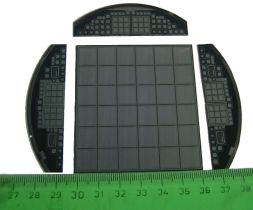 CALICE ECal employs silicon
diodes for detection of passage and measurement of the deposited
energy of passing charged particles. Sensor is manufactured on the 4
inch wafer with high resistivity, about 5 kΩcm. Silicon wafer is 525
μm thick.
CALICE ECal employs silicon
diodes for detection of passage and measurement of the deposited
energy of passing charged particles. Sensor is manufactured on the 4
inch wafer with high resistivity, about 5 kΩcm. Silicon wafer is 525
μm thick.
One wafer is a matrix of a 6
by 6 pads. One pad is 10x10 mm² large.
Wafer is slightly larger than 60 mm because of the included 1 mm guard
rings which safeguard surface currents and make electric field in the
active volume homogeneous on the border. About half of the wafers for
the CALICE ECal prototype was made by the On Semiconductor company in
Roznov in Czech republic.
Detection
Pads are p-n junction diodes
operated at reverse bias. This forms a sensitive region depleted of
mobile charge carriers and sets up an electric field that sweeps
charge liberated by a passage of radiation to the electrodes. High-resistivity
silicon is used for detector fabrication and therefore it is possible
to fully deplete the volume at voltages of about 150 to 200 V. When an
ionizing particle passes through, energy loss of just 3.6eV creates an
electron-hole pair. This is an order of magnitude less than energy
needed to produce electron-ion pair in gasses or about two orders of
magnitude less than energy necessary for production of a single photon
in scintillation counter. Passage of a minimum ionizing particle
through the fully depleted volume of the CALICE ECal prototype pad
should create about 42000 electron hole pairs. The read-out signal is
processed in the front end chips and converted to the digital form and
finally stored after a processing chain on the grid.
Mechanics
ECal prototype consists of 3
stacks, each has 10 layers of an alternating structure of tungsten and
silicon. Each stack has tungsten of different thickness: 1.4mm or 0.4
X0 per layer per for the stack, 2.8mm or 0.8 X0
for the layers in the second stack and 4.2mm or 1.2X0 for
the layers in the rear stack. This selection should guarantee a good
resolution at low energy due to the thinner tungsten at the front and
it should contain the electromagnetic showers well because of the
thick tungsten layers at the rear.
Silicon pads are mounted to
the PCBs by a mean of conductive glue. The signal is read out from a
single PCB using the FLC_PHY3 front end chips on the PCB which contain
input charge-sensitive preamplifier, signal shaper and a 18:1
multiplexer. Output is analog. The silicon wafers on each side of the
slab are staggered in the horizontal direction for the reasons of
avoiding alignment of guard rings.
[obrazok stacku]